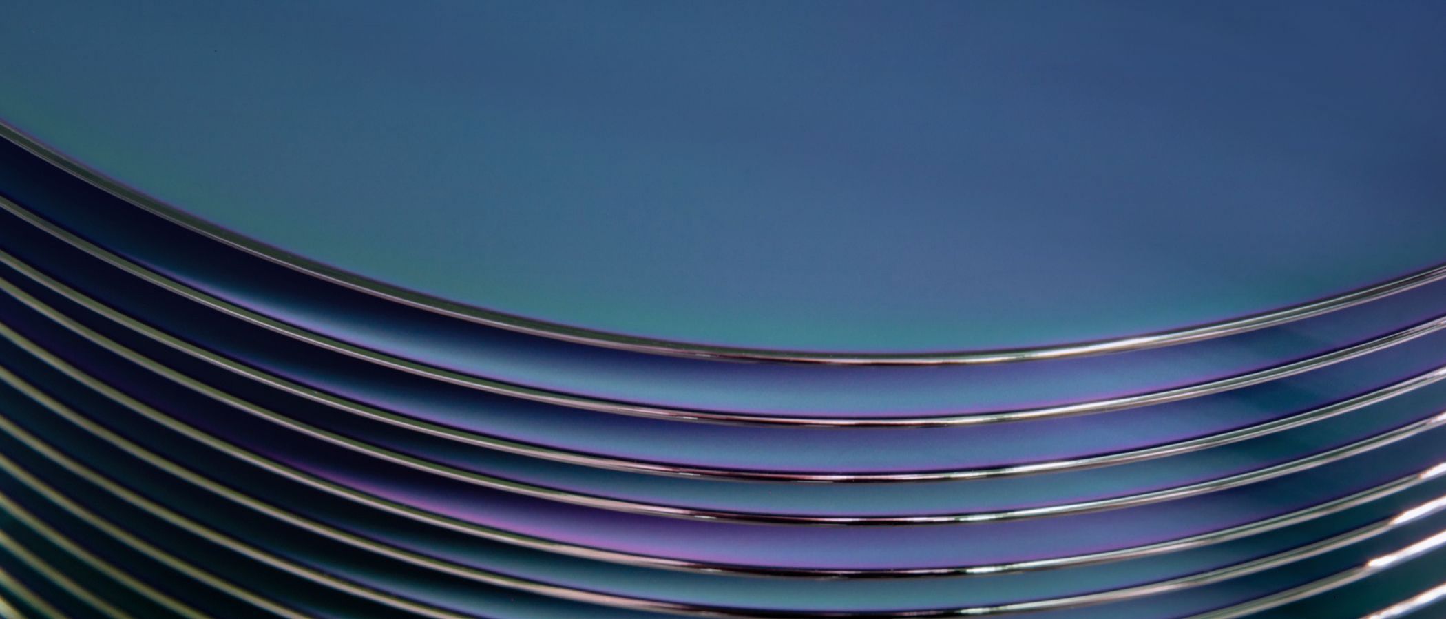

Epitaxy is one or more silicon single crystal layers growing on the polished wafer by chemical vapor deposition. The product parameters such as doping type, resistivity, thickness and lattice structure, etc., which all meet the requirements of specific devices with excellent uniformity and extremely low defect density.
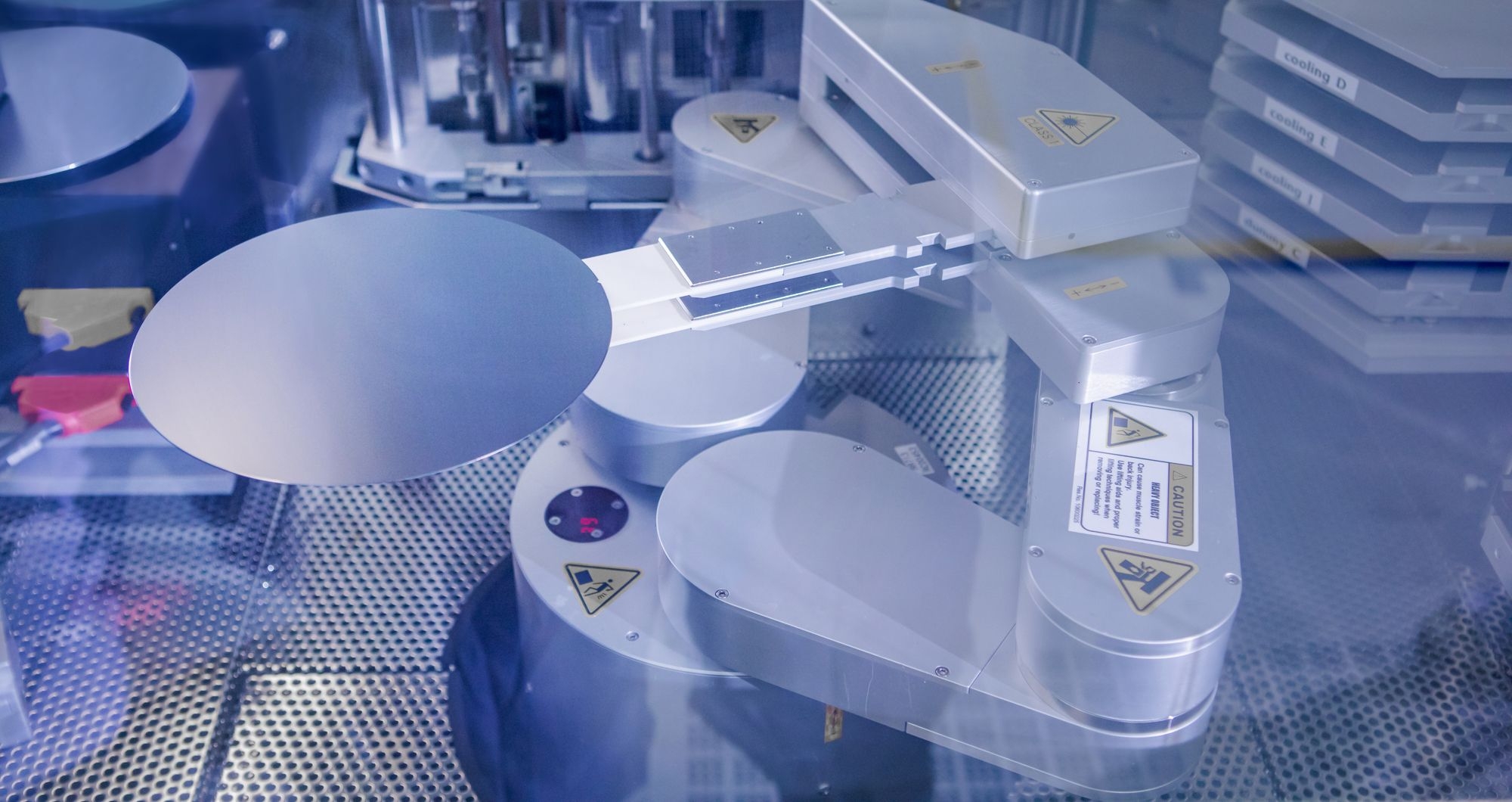
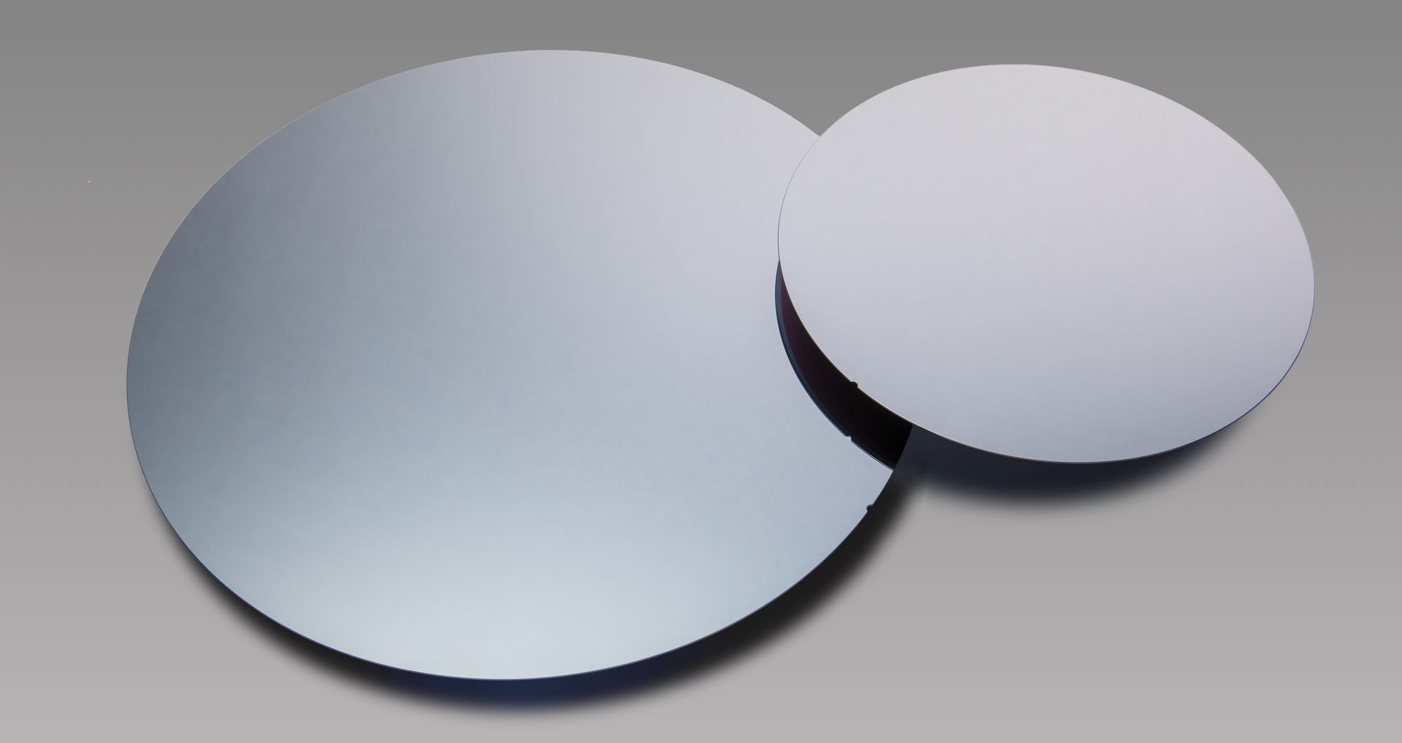
The semiconductor silicon epitaxial wafers of Wafer Works (Shanghai) Corporation (WWXS) are widely recognized by customers at home and abroad, gaining leading global market share. The integrated production of the products and the mastery of the three major technologies (crystal growth, silicon wafer molding and epitaxial growth) complement and reinforce each other to achieve the highest epitaxial quality. The technology of polished wafer makes a huge contribution to the Company’s competitiveness.
About Us
Wafer Works (Shanghai) Corporation (WWXS), formerly known as Shanghai Second Smelters Factory 901 founded by Shanghai Metallurgical Bureau in the 1960s, was the first production base for mass-produced integrated circuit silicon materials in China. In the 1990s, it was the first Chinese professional manufacturer that successfully exported semiconductor-grade silicon wafers to Europe and the Americas, and took the lead in stepping into the supply chain of the global silicon wafer market.
|
1
The first domestic supplier of integrated semiconductor epitaxial wafers
|
More than 20 years of industry experience
|
Supply to more than 35 countries
|
Served more than 3000 customers
|